



Semiconductor Spray Nozzles Manufacturer
We deliver ultra-pure spray nozzle systems for the semiconductor manufacturing industry. Our nozzles provide contamination-free performance in wafer wet cleaning, chemical mechanical polishing, photoresist development, etching processes, and ultra-pure water rinsing for advanced logic and memory device fabrication.
Industry Overview
The semiconductor manufacturing industry demands the highest purity spray technology preventing sub-nanometer contamination. Modern semiconductor fabs face challenges including removing particles as small as 10nm, delivering ultra-pure chemicals without contamination, maintaining Class 1-10 cleanroom environments, and processing 300mm wafers with atomic-level precision.
Spray nozzles are critical in wafer wet cleaning for pre-diffusion and post-etch particle removal, photolithography for developer and resist stripping, chemical mechanical polishing for slurry delivery and post-CMP cleaning, etching processes for wet chemical removal of films, and final wafer rinsing using 18 MΩ·cm ultra-pure water.
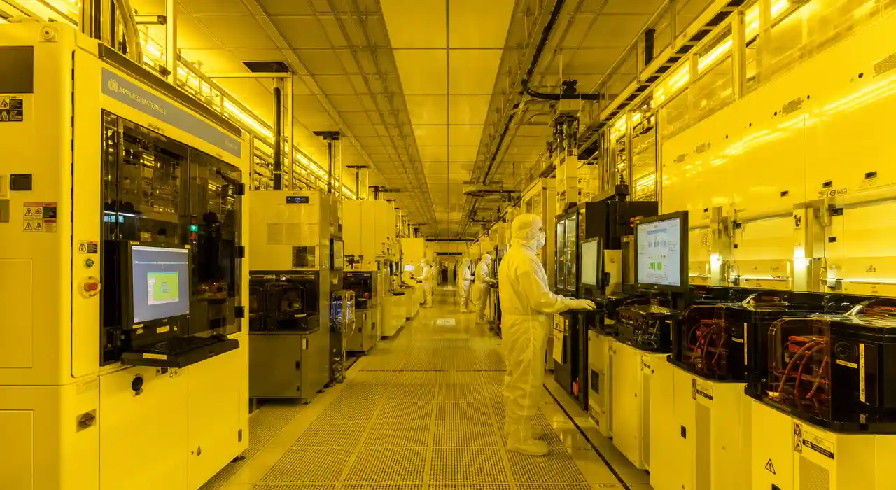
Semiconductor Production Process
Wafer Cleaning
RCA Clean, SC-1/SC-2, Particle Removal
Photolithography
Photoresist Development, Stripping
Etching
Wet Etch, Chemical Removal
CMP
Slurry Application, Post-CMP Cleaning
Deposition Cleaning
Pre-Deposition Clean, Chamber Cleaning
Final Rinse & Dry
Ultra-Pure Water Rinse, Spin Dry
Semiconductor Manufacturing Challenges & Solutions
Removing Sub-10nm Particles
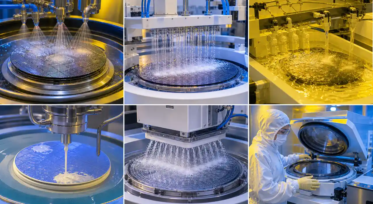
ChallengeAdvanced semiconductor nodes below 7nm require particle removal at sizes approaching single-digit nanometers. Particles as small as 10nm cause defects including shorts, opens, and parametric failures. Traditional immersion cleaning cannot generate sufficient force dislodging particles from high-aspect-ratio features including trenches and vias without damaging delicate structures.
SolutionOur precision spray nozzles deliver high-velocity ultra-pure water jets creating turbulent boundary layer flow dislodging sub-10nm particles, generate localized pressure pulses penetrating high-aspect-ratio structures, use PTFE and PFA materials with certified purity preventing particle shedding, and integrate with megasonic energy enhancing particle removal without mechanical damage. Spray-in-air processing eliminates cross-contamination between wafers present in immersion tanks.
View Cleaning & Washing Solutions →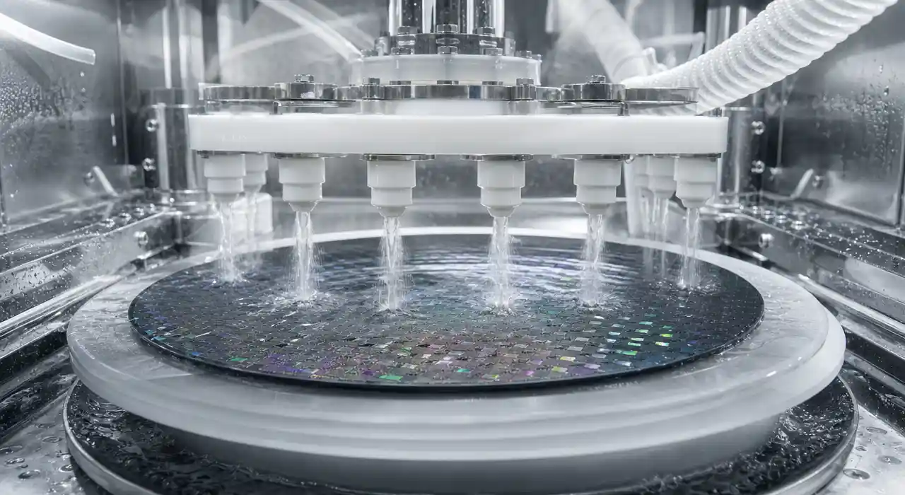
Preventing Metallic Contamination
ChallengeMetallic contamination at parts-per-trillion levels degrades device performance causing junction leakage, reduced carrier mobility, and reliability failures. Iron, copper, sodium, and other metals leaching from spray system materials contaminate wafers during wet processing. SEMI specifications limit metallic contamination below 1×10¹⁰ atoms/cm².
SolutionOur ultra-pure spray nozzles feature PTFE and PFA construction with documented metallic content below detection limits, undergo specialized cleaning and passivation preventing surface contamination, use virgin resins with certified purity from qualified suppliers, and include inline filtration with 0.003 micron membranes capturing particulate metals. All wetted components avoid metals entirely using high-purity fluoropolymers meeting SEMI standards for semiconductor wet processing.
View Product Materials →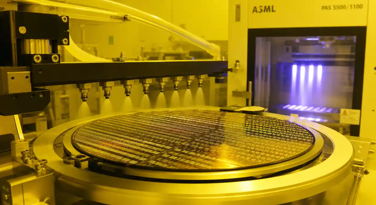
Achieving Uniform Chemical Distribution
ChallengeNon-uniform chemical distribution across 300mm wafers causes process variation affecting critical dimensions, film thickness, and etch profiles. Variations exceeding ±2% create yield-limiting defects. Center-to-edge uniformity and wafer-to-wafer repeatability determine production quality and device performance distributions.
SolutionOur semiconductor spray nozzles deliver precision full cone patterns with ±1% uniformity across 300mm diameter, maintain consistent flow rates through automated pressure compensation, feature optimized orifice designs validated through computational fluid dynamics, and integrate with robotic wafer handling providing repeatable positioning. Multiple nozzle arrays with sequential spray timing ensure complete coverage without chemical waste.
View Surface Treatment Solutions →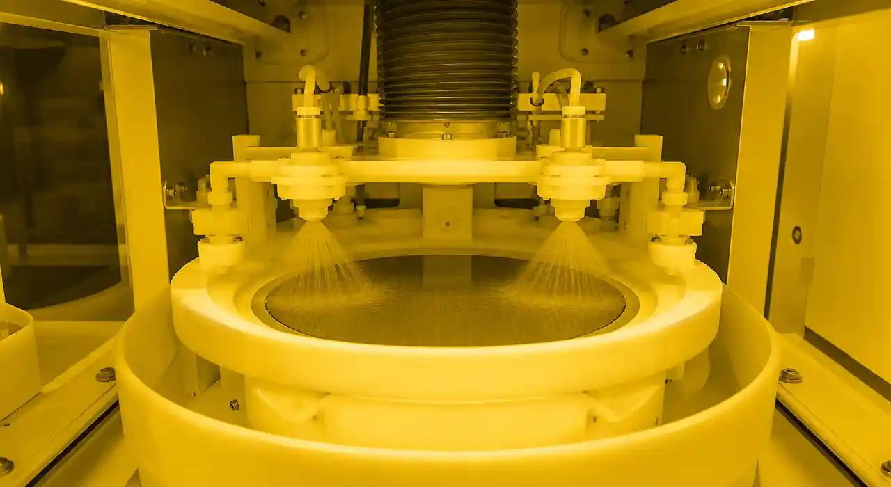
Maintaining Class 1 Cleanroom Standards
ChallengeAdvanced semiconductor fabs require Class 1 cleanrooms (ISO 3) with particle counts below 10 particles/m³ at 0.1 microns. Spray systems generate aerosols potentially carrying contamination. Any particle shedding from nozzle materials or bacterial growth in fluid systems compromises yields. Outgassing organic compounds adsorb on wafer surfaces affecting lithography and film deposition.
SolutionOur cleanroom-certified spray nozzles feature electropolished fluid passages eliminating particle-trapping crevices, use virgin PTFE and PFA materials with certified low outgassing meeting SEMI specifications, undergo Class 10 cleanroom assembly and 100% particle inspection, and include bacterial barrier filters preventing microbial contamination. Low-pressure spray minimizes aerosol generation maintaining cleanroom particle counts during operation.
View Cleanroom Solutions →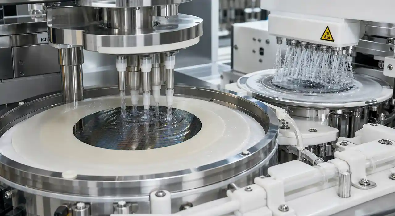
Reducing Ultra-Pure Water Consumption
ChallengeSemiconductor fabs consume enormous quantities of 18 MΩ·cm ultra-pure water with production costs of $1-5 per cubic meter including energy for purification, heating, and chilling. Typical fab water consumption of 6-10 million liters daily represents $2-15 million annual operating expense. Environmental regulations pressure water usage reduction.
SolutionOur optimized spray systems reduce UPW consumption by 40-60% compared to immersion processing through precision flow control delivering exact quantities required for particle removal, high-velocity spray patterns replacing immersion baths with fraction of volume, closed-loop recycling systems filtering and reusing rinse water, and multi-stage rinsing with counter-current flow minimizing fresh UPW usage. Spray processing delivers superior cleaning effectiveness while dramatically reducing water volume.
View Automatic Spray Systems →Semiconductor Application Example
300mm Wafer Post-CMP Cleaning Optimization
Problem: A logic device manufacturer experienced yield loss from residual slurry particles and copper contamination after CMP. Immersion scrubber cleaning required 8-minute cycles consuming 300 liters UPW per wafer batch. Defect density of 0.18/cm² exceeded yield targets. Metallic contamination approached SEMI specification limits.
Solution: Designed spray-based post-CMP cleaning system with high-pressure PFA nozzles delivering 18 MΩ·cm UPW in counter-rotating spray pattern. Implemented three-stage process: initial slurry rinse, dilute chemical clean, and final UPW rinse with megasonic assist. Upgraded all wetted components to certified ultra-pure PFA and PTFE materials. Added inline conductivity monitoring and particle counting.
Results:
- Defect density reduced to below 0.05/cm² meeting advanced node yield requirements
- Cleaning cycle time reduced from 8 minutes to 3.5 minutes increasing tool throughput
- UPW consumption reduced by 55% through spray processing
- Metallic contamination levels improved 10x meeting tighter specifications
Why Choose Us for Semiconductor Spray Systems
Industry Experience
Certified Purity
Spray Uniformity
Cleanroom
Recommended Nozzle Solutions
PTFE Ultra-Pure Nozzle
Application: Wafer cleaning, ultra-pure water delivery, chemical processing
View Details →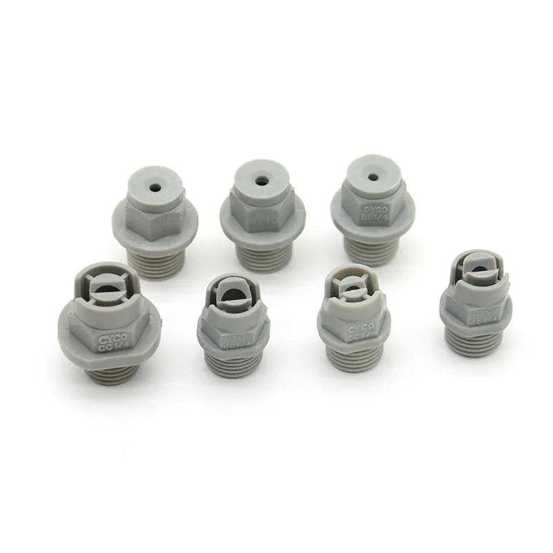
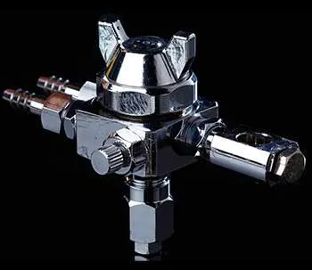
PVDF Chemical Resistant Nozzle
Application: Acid/base delivery, chamber cleaning, general wet processing
View Details →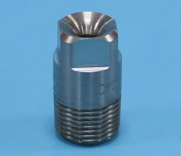
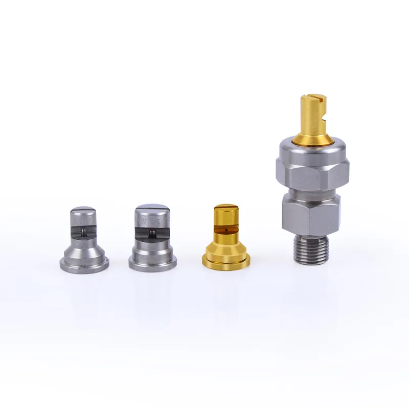
CC Flat Fan Spray Nozzle
Application: Linear spray coverage, rinse applications (316L SS option)
View Details →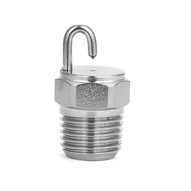
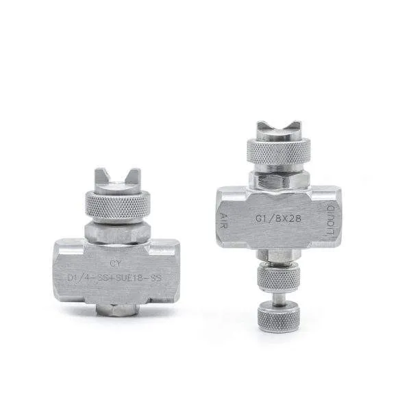
Anti-Drip Atomizing Nozzle
Application: Chemical delivery preventing contamination from drips
View Details →Frequently Asked Questions
Semiconductor manufacturing uses ultra-pure spray nozzles engineered for contamination-free processing. Wafer wet cleaning requires PTFE or PFA full cone nozzles delivering SC-1, SC-2, and dilute HF chemistries with uniform distribution across 300mm wafers. Post-CMP cleaning uses high-pressure ultra-pure water spray nozzles removing slurry particles and metallic residues. Photoresist development employs precision flat fan nozzles applying developer solutions with controlled flow rates. Chamber cleaning systems use chemically-resistant nozzles delivering aggressive chemistries removing deposited films. All semiconductor nozzles must prevent metallic leaching below 1 ppb, eliminate particle shedding below 0.1 microns, resist chemical attack from concentrated acids and bases, maintain 18 MΩ·cm ultra-pure water resistivity, and meet SEMI material standards. Cleanroom Class 10 assembly and certification documentation ensure contamination-free operation in advanced fabs.
Yes, we specialize in SEMI-certified spray nozzles meeting semiconductor industry purity standards. Our nozzles feature virgin PTFE and PFA materials from qualified suppliers with documented metallic content below 1 ppb including iron, copper, sodium, and other trace metals. All wetted components undergo specialized cleaning procedures including solvent degreasing, aqua regia passivation, and ultra-pure water rinsing before Class 10 cleanroom assembly. We provide comprehensive documentation including material purity certificates with ICP-MS analysis results, particle generation test reports to SEMI F57 standards, ionic contamination testing showing resistivity maintenance above 18 MΩ·cm, chemical compatibility validation for semiconductor chemistries, and outgassing analysis meeting SEMI specifications. Lot traceability enables material genealogy tracking required by semiconductor quality systems. Our SEMI-certified nozzles integrate into wafer wet processing tools, spray acid hoods, and automated cleaning systems meeting advanced node contamination requirements.
Semiconductor chemical processing requires specialized fluoropolymer materials. PTFE (polytetrafluoroethylene) offers universal chemical resistance to all semiconductor chemistries including concentrated HF, H2SO4, HCl, NH4OH, and organic solvents with temperature capability to 260°C and the lowest metallic leaching of any material. PFA (perfluoroalkoxy) provides similar chemical resistance with improved mechanical properties, transparency enabling visual inspection, and superior surface finish reducing particle traps. PVDF (polyvinylidene fluoride) resists most acids and bases at lower cost than PTFE/PFA suitable for less critical applications. Materials NOT suitable for semiconductor processing include stainless steel (metallic leaching), acetal plastics (chemical attack), PEEK (organic outgassing), and any elastomers (particle shedding and leachables). All semiconductor nozzles require virgin resin materials with certified purity, specialized cleaning and passivation, and cleanroom assembly preventing contamination introduction. We provide chemical compatibility data and contamination testing for all materials validating semiconductor fab compatibility.
Yes, we provide replacement spray nozzles for semiconductor wet processing tools from all manufacturers. Our engineering team works with fab process engineers evaluating current system performance through particle removal efficiency testing, metallic contamination analysis using ICP-MS, spray uniformity measurement across test wafers, and chemical consumption audits. We document existing nozzle specifications including materials, connections, flow rates, and spray patterns. We offer direct replacements maintaining tool interfaces while upgrading to improved purity materials, optimized spray patterns reducing chemical usage, or enhanced durability extending service intervals. For wet bench retrofits, we provide complete spray manifold assemblies designed for specific wafer handling systems with validated cleaning performance. Installation services include cleanroom procedures, tool qualification testing, and documentation package supporting fab change control systems. Most semiconductor nozzle upgrades achieve improved yields through better contamination control, reduced consumable costs from optimized spray patterns, and extended tool uptime from superior reliability.
Semiconductor fabs achieve 40-60% UPW reduction through spray processing optimization. First, replace immersion cleaning baths with spray-in-air systems delivering high-velocity UPW jets removing particles with 5-10% of immersion volume. Implement multi-stage counter-current rinsing where final rinse UPW becomes initial rinse input reducing fresh water requirements. Upgrade to precision spray nozzles with optimized patterns eliminating waste from overspray or inadequate coverage. Install closed-loop recycling systems filtering used rinse water to 0.003 microns and reconditioning to 18 MΩ·cm for reuse in pre-rinse stages. Add real-time conductivity monitoring adjusting rinse duration based on actual contamination removal rather than fixed time cycles. Optimize spray nozzle positioning and flow rates through computational modeling minimizing water volume while maintaining particle removal effectiveness. Use dry processing alternatives including vapor-phase cleaning where applicable. Typical UPW savings of 2-5 million liters daily represent $500,000 to $6 million annual cost reduction for 300mm fabs with payback periods of 12-24 months on spray system investments.
Semiconductor spray nozzle maintenance requires stringent cleanroom procedures preventing contamination introduction. PTFE and PFA nozzles in UPW service typically require quarterly inspection for particle buildup or film deposition with ultrasonic cleaning in dilute acid or base followed by UPW rinsing. Chemical delivery nozzles need monthly inspection for chemical deposits or material degradation with replacement when spray patterns deteriorate or flow rates deviate from specifications. Metallic contamination monitoring through wafer testing or inline sensors indicates when nozzle replacement is required typically annually in critical applications. All maintenance uses Class 100 cleanroom procedures with documented cleaning protocols, ESD-safe handling preventing static discharge, and double-bagged cleanroom packaging for spare parts. Preventive replacement schedules based on process cycles or time intervals prevent contamination excursions from degraded nozzles. Quick-disconnect fittings enable tool-free nozzle changes during scheduled PM intervals. We provide maintenance training specific to semiconductor cleanroom practices, validated cleaning procedures for nozzle refurbishment, and technical support for contamination troubleshooting including material analysis and replacement recommendations.